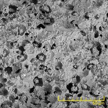
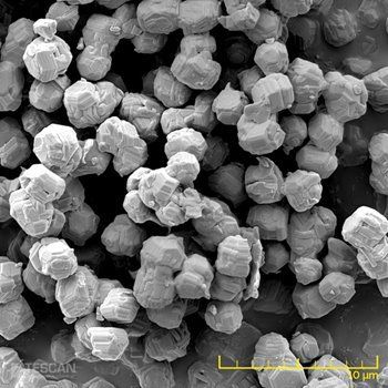
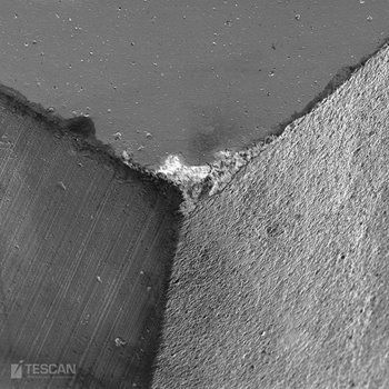
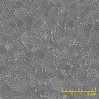
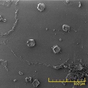
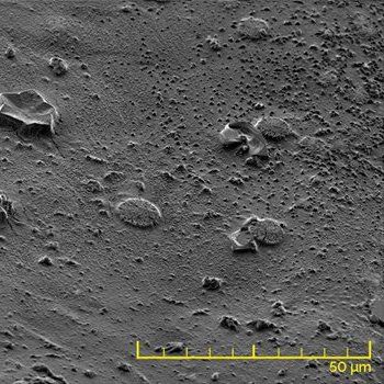
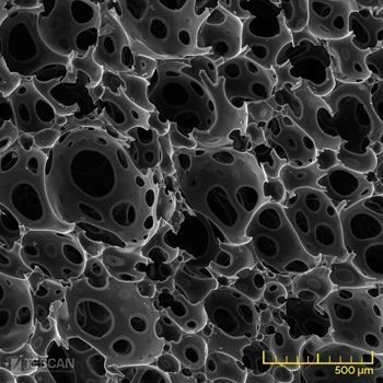
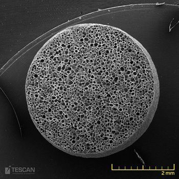
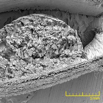
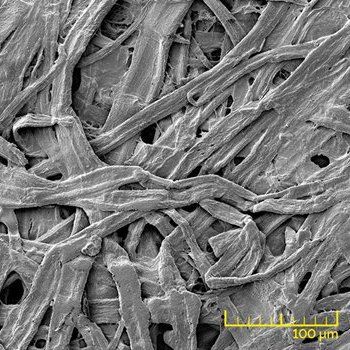
Materials Science is a field which deals with the discovery and development of new materials and methods for their study. It is a multidisciplinary science involving different fields of knowledge such as physics, chemistry and engineering. Materials Science focuses on studying the most important characteristics of materials such as their mechanical, chemical, electrical, thermal, optical and magnetic properties. The field can be sub-divided into different disciplines including nanomaterials, organic materials, electronic/photonic materials, structural/composite materials and smart materials.
Steels and metal alloys
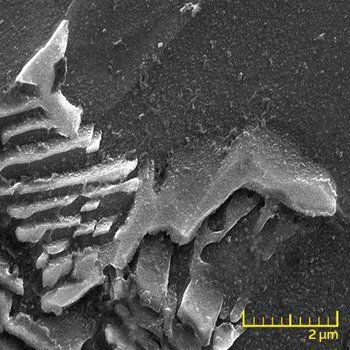
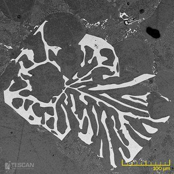
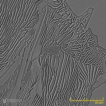
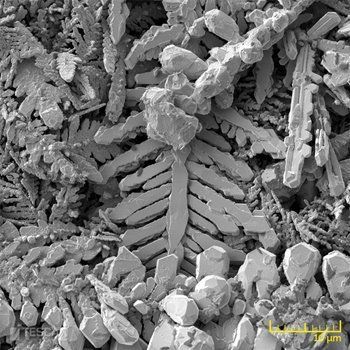
High resolution and large depth of focus are the main functions which make scanning electron microscope (SEM) a great tool for observing topographic features of samples made of steel and metal alloys.
Slide title
Contact layers under a solder ball imaged at 5 keV with the InBeam SE detector for topographic contrast (left), and the In-Beam f-BSE detector for material contrast (right).
Button
Slide title
Contact layers under a solder ball imaged at 5 keV with the InBeam SE detector for topographic contrast (left), and the In-Beam f-BSE detector for material contrast (right).
Button
Slide title
The beam deceleration improves imaging at low landing energies. Surface features in an Al flake become visible only at a landing energy of 500 eV (right). The multi-detector system enables simultaneous detection of BSE (left) and SE (right) signals.
Button
Slide title
The beam deceleration improves imaging at low landing energies. Surface features in an Al flake become visible only at a landing energy of 500 eV (right). The multi-detector system enables simultaneous detection of BSE (left) and SE (right) signals.
Button
Slide title
Image of an anode surface doped with Pt nanoparticles.
Button
Ceramics and hard coatings
Uncoated and non-conducting samples can be observed in the variable pressure mode without damaging the sample. Components made of ceramic materials are in some cases the only solution to technical problems that cannot be resolved with conventional materials.
Slide title
Contact layers under a solder ball imaged at 5 keV with the InBeam SE detector for topographic contrast (left), and the In-Beam f-BSE detector for material contrast (right).
Button
Slide title
Contact layers under a solder ball imaged at 5 keV with the InBeam SE detector for topographic contrast (left), and the In-Beam f-BSE detector for material contrast (right).
Button
Slide title
The beam deceleration improves imaging at low landing energies. Surface features in an Al flake become visible only at a landing energy of 500 eV (right). The multi-detector system enables simultaneous detection of BSE (left) and SE (right) signals.
Button
Slide title
The beam deceleration improves imaging at low landing energies. Surface features in an Al flake become visible only at a landing energy of 500 eV (right). The multi-detector system enables simultaneous detection of BSE (left) and SE (right) signals.
Button
Slide title
Image of an anode surface doped with Pt nanoparticles.
Button
Glass
TESCAN SEMs are of great benefit to the glass industry. Glass and its derived products are an important part of automotive, construction, engineering and energy industry, among others.
Slide title
Contact layers under a solder ball imaged at 5 keV with the InBeam SE detector for topographic contrast (left), and the In-Beam f-BSE detector for material contrast (right).
Button
Slide title
Contact layers under a solder ball imaged at 5 keV with the InBeam SE detector for topographic contrast (left), and the In-Beam f-BSE detector for material contrast (right).
Button
Slide title
The beam deceleration improves imaging at low landing energies. Surface features in an Al flake become visible only at a landing energy of 500 eV (right). The multi-detector system enables simultaneous detection of BSE (left) and SE (right) signals.
Button
Slide title
The beam deceleration improves imaging at low landing energies. Surface features in an Al flake become visible only at a landing energy of 500 eV (right). The multi-detector system enables simultaneous detection of BSE (left) and SE (right) signals.
Button
Slide title
Image of an anode surface doped with Pt nanoparticles.
Button
Polymers and Composites
High resolution and large depth of focus are capabilities that make TESCAN SEMs excellent instruments to observe polymers, plastic and other composite materials.
Slide title
Contact layers under a solder ball imaged at 5 keV with the InBeam SE detector for topographic contrast (left), and the In-Beam f-BSE detector for material contrast (right).
Button
Slide title
Contact layers under a solder ball imaged at 5 keV with the InBeam SE detector for topographic contrast (left), and the In-Beam f-BSE detector for material contrast (right).
Button
Slide title
The beam deceleration improves imaging at low landing energies. Surface features in an Al flake become visible only at a landing energy of 500 eV (right). The multi-detector system enables simultaneous detection of BSE (left) and SE (right) signals.
Button
Slide title
The beam deceleration improves imaging at low landing energies. Surface features in an Al flake become visible only at a landing energy of 500 eV (right). The multi-detector system enables simultaneous detection of BSE (left) and SE (right) signals.
Button
Slide title
Image of an anode surface doped with Pt nanoparticles.
Button
Material for building and civil engineering
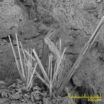
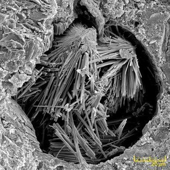
Scanning electron microscopy has been an essential analytical technique for studying a variety of construction materials.
Slide title
Contact layers under a solder ball imaged at 5 keV with the InBeam SE detector for topographic contrast (left), and the In-Beam f-BSE detector for material contrast (right).
Button
Slide title
Contact layers under a solder ball imaged at 5 keV with the InBeam SE detector for topographic contrast (left), and the In-Beam f-BSE detector for material contrast (right).
Button
Slide title
The beam deceleration improves imaging at low landing energies. Surface features in an Al flake become visible only at a landing energy of 500 eV (right). The multi-detector system enables simultaneous detection of BSE (left) and SE (right) signals.
Button
Wood, Textile and Paper
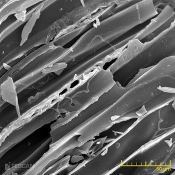
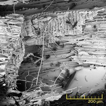
Scanning electron microscopy has been an essential analytical technique for studying a variety of construction materials.
Slide title
Contact layers under a solder ball imaged at 5 keV with the InBeam SE detector for topographic contrast (left), and the In-Beam f-BSE detector for material contrast (right).
Button
Slide title
Contact layers under a solder ball imaged at 5 keV with the InBeam SE detector for topographic contrast (left), and the In-Beam f-BSE detector for material contrast (right).
Button
Slide title
The beam deceleration improves imaging at low landing energies. Surface features in an Al flake become visible only at a landing energy of 500 eV (right). The multi-detector system enables simultaneous detection of BSE (left) and SE (right) signals.
Button
Slide title
The beam deceleration improves imaging at low landing energies. Surface features in an Al flake become visible only at a landing energy of 500 eV (right). The multi-detector system enables simultaneous detection of BSE (left) and SE (right) signals.
Button
Slide title
Image of an anode surface doped with Pt nanoparticles.
Button
Need more information?
Subscribe to our newsletter
Thanks for contacting us. We will respond as soon as possible
There was an error sending your message. Try it later