TESCAN SOLARIS X
A Plasma FIB-SEM platform for deep sectioning and
the highest resolution end-pointing for package level
failure analysis
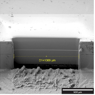
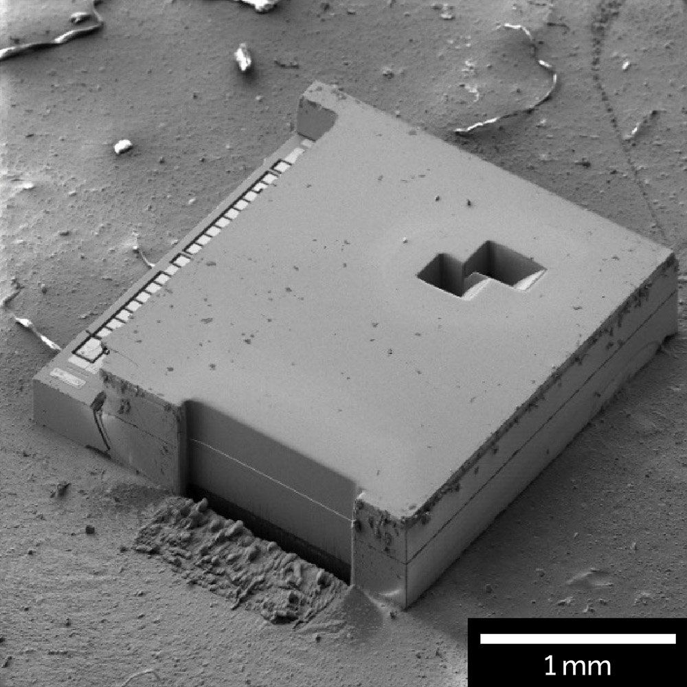
- Curtaining-free large-area cross-sectioning for physical failure analysis of advanced packaging technologies.
- Prepare large area FIB-cross-sections up to 1 mm wide.
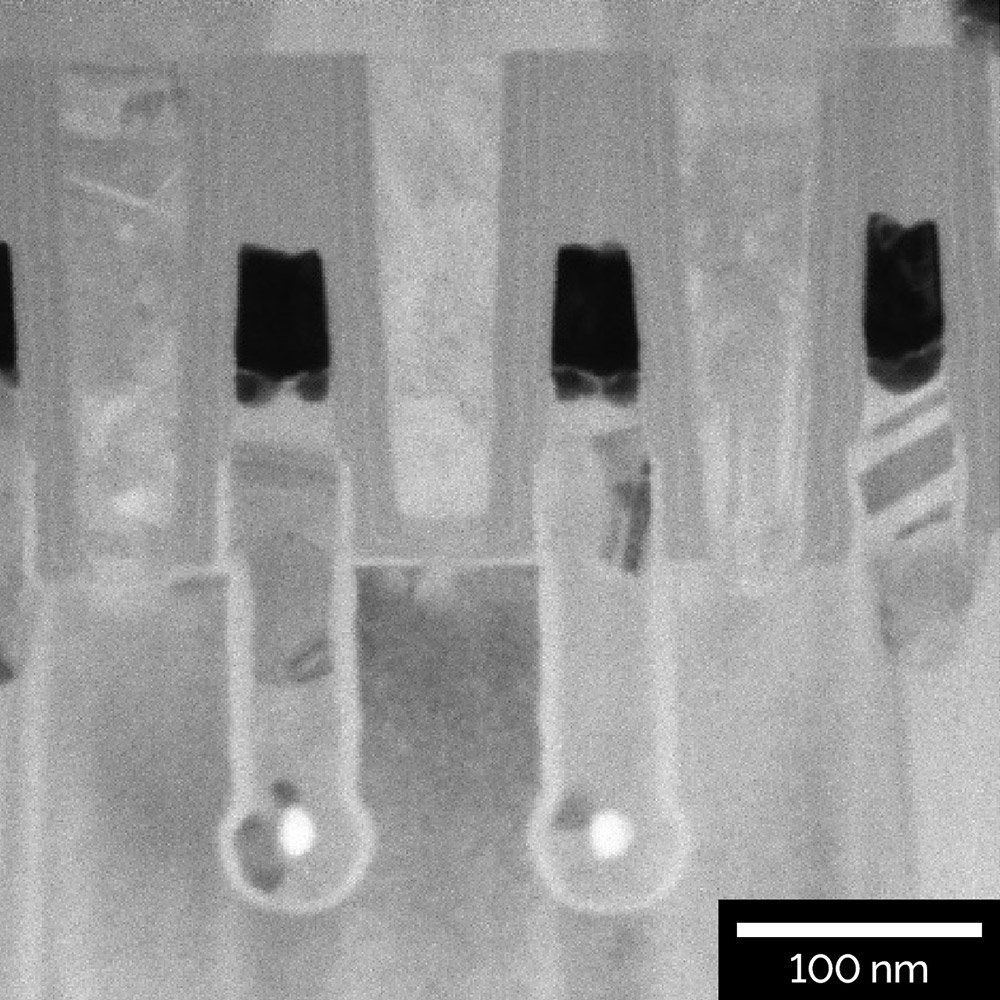
- Obtain low noise, high-resolution image at low keVs in short acquisition time at FIB-SEM coincidence with the sample tilted.
- Live SEM-monitoring during FIB milling for precise end-pointing.
- Observe the most beam-sensitive materials using low keVs ultra-high resolution for surface sensitivity and high material contrast.
- Effective techniques and recipes for fast and artefact-free cross-sectioning of composite samples (OLED and TFT displays, MEMS devices, isolation dielectrics) at high currents
- Essence™ easy-to-use modular user interface