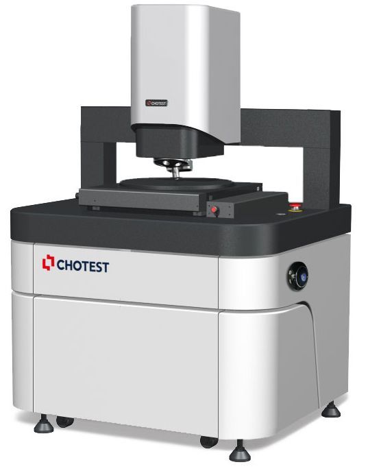

SuperView W1
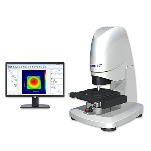
The SuperView W1 Nano 3D Optical Surface Profilometer from Chotest Technology Inc. is an advanced optical measurement system designed for three-dimensional surface analysis with nanometer resolution. It utilizes interferometry and non-contact measurement technology to accurately capture the topography, roughness, and microgeometry of materials and components.
Thanks to its high acquisition speed and powerful 3D analysis software, the SuperView W1 provides highly reliable, detailed surface maps and metrological parameters. It is an ideal solution for applications in microelectronics, semiconductors, optics, advanced materials, and quality control in high-precision manufacturing processes.
- Standard field of view: (0.98*0.98) mm
- Scanning range: ≤10 mm
- Resolution: 0.1 nm
- Scenario measurement accuracy: 0.3%
- Repeatability of the stage measurement: 0.08% 1σ
Applications
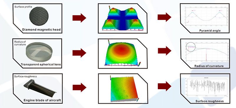
The SuperView W1 3D optical surface profilometer is an ideal instrument for sub-nanometer measurements of various precision parts. Based on the principle of white light interference technology, combined with a precision Z-direction scanning module and a 3D modeling algorithm, it non-contactly scans the object's surface and generates a 3D image. After processing and analysis of the 3D image by the XtremeVision software, a series of 2D and 3D parameters are obtained, reflecting the surface quality of the object. The SuperView W1 is an easy-to-use precision optical instrument with powerful analysis functions for all types of surface shape and roughness parameters. Thanks to its unique light source, it can measure various precision parts with both smooth and rough surfaces.
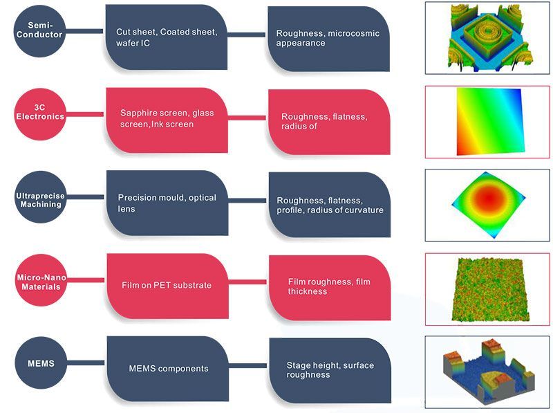
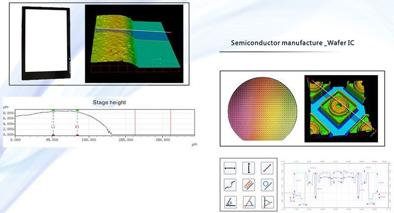
Measurement and analysis of the surface shape and profile characteristics of various products, components and materials, such as flatness, roughness, waviness, appearance, surface defects, abrasion, corrosion, gaps, holes, stages, curvature, deformation, etc.
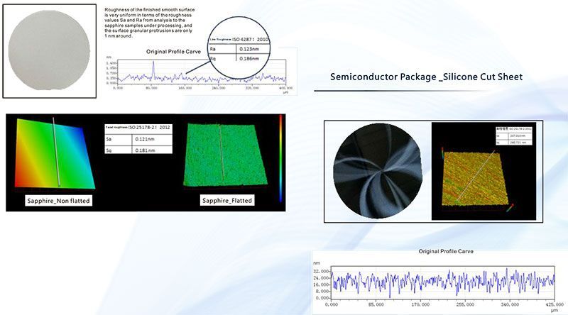
3C Electronics - Sapphire Crystal
| Features | |
|---|---|
| Model No. | SuperView W1 |
| Light source | LED blanco |
| Video system | 1024×1024 |
| Objective lens | Standard: 10X (optional: 2.5X, 5X, 20X, 50X, 100X) |
| Optical zoom | Standard: 0.5X Optional: 0.375X, 0.75X, 1X |
| Standard field of view | 0,98 × 0,98 mm |
| Lens turret | Standard: 3-hole manual turret (Optional: 5-hole motorized turret) |
| XY object table | Size 320×200 mm |
| Moving range 140×100 mm | |
| Load capacity 10 kilos | |
| Control Method - Motorized | |
| Tilt (manual) | ±4° |
| Z-axis focus | Travel range 100 mm |
| Control Method - Motorized | |
| Z-stroke scan range | 10 mm |
| Repeatability of surface shape* | 0,1 nm |
| RMS Roughness Repeatability* | 0,005 nm |
| Step height measurement* | Accuracy: 0.3%; Repeatability: 0.08%(1σ) |
| Scanning speed at a resolution of 0.1 nm | 1,85 μm/s |
| Weight | 140 kg |
| Size (length x width x height) | 700x606x920mm |
| Stage measurement | Temperature 0 °C ~ 30 °C, fluctuation <2 °C/60 min |
| Humidity 5%~95% RH, non-condensing | |
| Vibration VC-C or better | |
| Software noise assessment * 3σ≤4 nm | |
| Compressed air 0.6 MPa, oil-free, water-free, 6 mm hose diameter | |
| AC power supply 100~240 V, 50/60 Hz, 4 A, 300 W | |
| Other - No strong magnetic field, no corrosive gas |
Note:
* 1 Use EPSl mode to measure the 0.2 nm Sa silicon wafer in a laboratory environment; single-line 80 µm filter for a full field of view
* 2 Measure the 0.2 nm Sa silicon wafer in a laboratory environment according to ISO 25178.
* 3 Measure the standard 5 µm step height block in a laboratory environment according to ISO 1060-1:2000* 4 When the software noise assessment is 4 nm ≤ 3 σ ≤ 10 nm, the RMS repeatability of roughness is revised to 0.015 nm, the accuracy of the step height measurement is revised to 0.7%, and the repeatability of the step height measurement is revised to 0.12%; When the software noise assessment is 3 σ> 10 nm, the environment does not meet the equipment usage requirement and the site needs to be changed.
| Parameters | |
|---|---|
| Standard | |
| ISO 4287-1997 | |
| A>amplitude | Main section - Pp, Pv, Pz, PC, Pt, Pa, Pq, Psk, Pku |
| Aspereza - Rp, Rv, Rz, Rc, Rt, Ra, Rq, Rsk, Rku | |
| W>aviness - Wp, Wv, Wz, Wc, Peso, Wa, Wq, Wsk, Wku | |
| interval | Main section - PSm, Pdq |
| Aspereza - RSm, Rdq | |
| W>aviness - WSm,Wdq | |
| S>substance | Main section - Pmr, Pdc |
| Aspereza - Rmr, Rdc, Rmr(Rz/4) | |
| IN | |
| Top | Main section - PPc |
| Aspereza - RPc | |
| IN | |
| ISO 13565 | ISO 13565-2 Rk, Rpk, Rvk, Mr1, Mr2, A1, A2, Rpk, Rvk |
| ISO 12085 | Roughness graph - R, AR, R×, No |
| Gráfico de W>aviness> - W,AW,W×,Wte | |
| Another graph - Rke, Rpke, Rvke | |
| AMS >B46.1 | 2D - Rt, Rp, Rv, Rz, Rpm, Rma×, Ra, Rq, Rsk, Rku, tp, Htp, Pc, Rda, Rdq, RSm, Peso |
| DIN EN ISO 4287-2010 | Perfil original - Pa, Pq, Pp, Pv, Pz, Pc, Pt, PSk, PKu, PSm, PPc, Pdq, Pdc, Pmr, |
| Aspereza - Ra,Rq,Rp,Rv,Rz,Rc,Rt,RSk,RKu,RSm,RPc,Rdq,Rdc,Rmr | |
| W>aviness - Wa,Wq,Wp,Wv,Wz,Wc,Wt,WSk,WKu,WSm,WPc,Wdq,Wdc,Wmr | |
| Standard JIS B0601-2013 | Perfil original - Pa, Pq, Pp, Pv, Pz, Pc, Pt, PSk, PKu, PSm, PPc, Pdq, Pdc, Pmr, |
| Aspereza - Ra,Rq,Rp,Rv,Rz,Rc,Rt,RSk,RKu,RSm,Rdq,Rdc,Rmr | |
| W>aviness - Wa,Wq,Wp,Wv,Wz,Wc,Wt,WSk,WKu,WSm,WPc,Wdq,Wdc,Wmr | |
| GBT 3505-2009 | Perfil original - Pa, Pq, Pp, Pv, Pz, Pc, Pt, PSk, PKu, PSm, PPc, Pdq, Pdc, Pmr, |
| Aspereza - Ra,Rq,Rp,Rv,Rz,Rc,Rt,RSk,RKu,RSm,Rdq,Rdc,Rmr | |
| W>aviness - Wa,Wq,Wp,Wv,Wz,Wc,Wt,WSk,WKu,WSm,WPc,Wdq,Wdc,Wmr |
| 3D parameters | |
|---|---|
| Standard | |
| ISO 25178 | Height - Cuadrado, Ssk, Sku, Sp, Sv, Sz, Sa |
| Function - Smr,Smc,S×p | |
| Space - Exit, Street, Standard | |
| Composite parameters - Sdq,Sdr | |
| Volumen - Vm, Vv, Vmp, Vmc, Vvc, Vvv | |
| Form - Spd, Spc, S10z, S5p, S5V, SDA, Sha, SdV, Shv | |
| Functional - Sk, Spk, Svk, Smr1, Smr2, Spq, Svq, Smq | |
| ISO 12781 | Plain - FLTt,FLTp,FLTv,FLTq |
| EUR 15178N | Amplitude - Sa, Cuadrado, Talla, Ssk, Sku, Esp, Sv, St |
| Space - Str,Std,Sal | |
| Composite parameters - Sdq, Sds, Ssc, Sdr, Sfd | |
| Area, Volume - Smr,Sdc | |
| Function - Sc, Spk, Svk, Sr1, Sr2, Spq, Svq, Smq | |
| Functional - Sbi, Sci, Svi | |
| EUR 16145 Y | Amplitud - SaSq, Sy, Sz, Ssk, Sku |
| Mixed parameters - Ssc,Sdq | |
| Functional - Sbi, Science | |
| Space - Sdsrw | |
| Dureza - Hs,Hvol | |
| ASME B46.1 | 3D - St,Sp,Sv,Sq,Sa,Ssk,Sku,SWt |
You may also be interested in: