


Semiconductores
La Microscopía Electrónica de Barrido (MEB) en combinación con haces de iones enfocados (FIB), es una técnica que ofrece una amplia variedad de análisis con altos niveles de precisión ideales pare seguir el ritmo de la rápida evolución de la industria de los semiconductores.
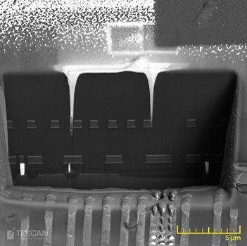
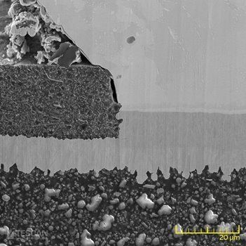
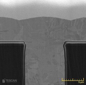
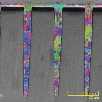
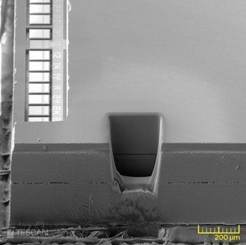
Análisis de fallos en circuitos integrados
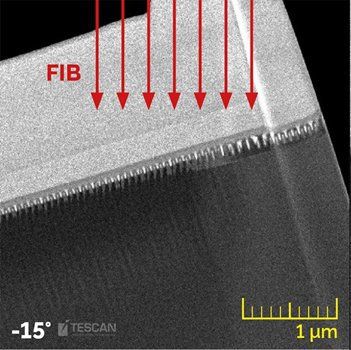
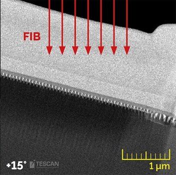
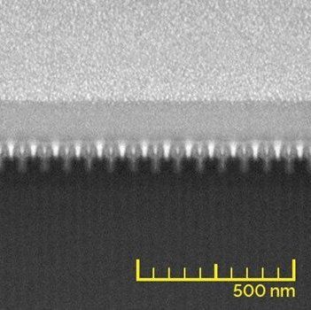
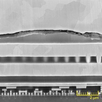
La industria de los semiconductores continúa reduciendo el tamaño de los dispositivos electrónicos. Actualmente, la tecnología punta está basada en circuitos integrados con procesos de fabricación de 14 y 10 nm y con la tecnología de nodos de 7 nm aún en etapa de desarrollo pero muy cerca de su comercialización. TESCAN ofrece una serie completa de microscopios, instrumentos y accesorios que son ideales para el análisis de fallos en los circuitos integrados de última generación.
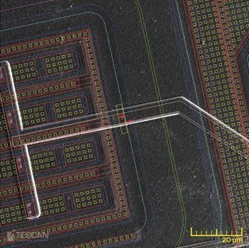
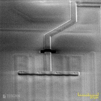
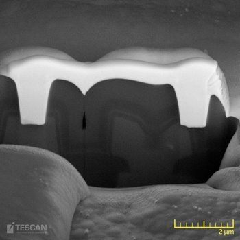
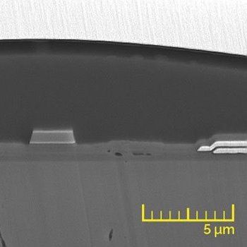
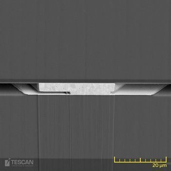
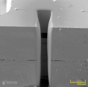
Modificación de Circuitos
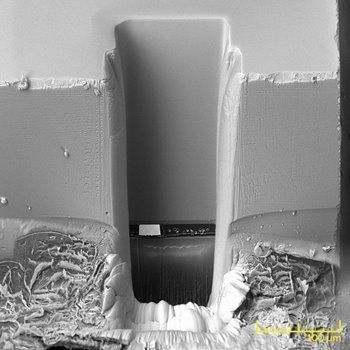
La modificación de circuitos es una técnica común utilizada en la fase de diseño-depuración de circuitos integrados. La mayoría de estas aplicaciones se realizan mediante sistemas FIB equipados con un Sistema de Inyección de Gas (GIS). Esta combinación permite el fresado y eliminación muy precisa de material en sitios específicos, así como la deposición de contactos conductores o aislantes.
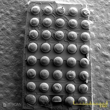
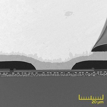
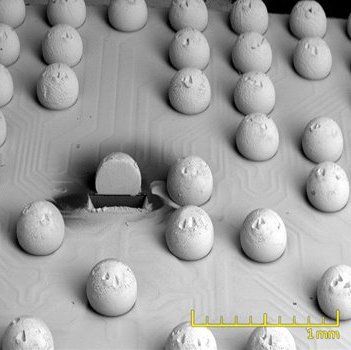
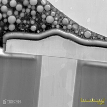
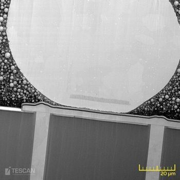
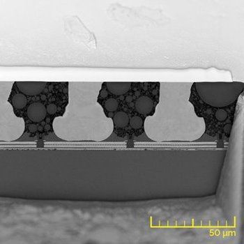
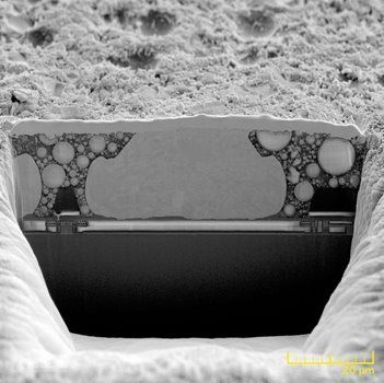
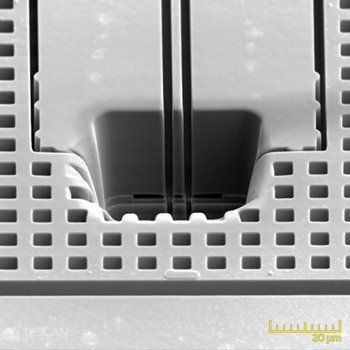
Matriz de rejilla de bolas (BGA)
Es una tecnología de empaquetado de chips que consiste en una disposición de bolas de soldadura localizada en la parte inferior de un paquete de chips. Las BGA se han desarrollado como una respuesta a la tendencia que existe en la industria de los semiconductores hacia la miniaturización de circuitos integrados y cuyo objetivo es una mayor integración, mayor densidad y mejor funcionalidad.
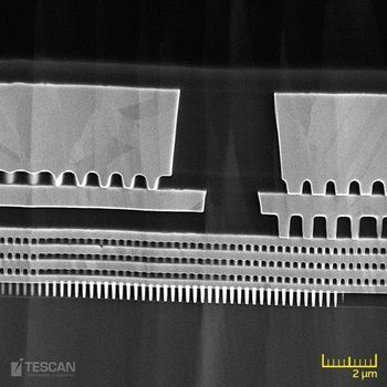
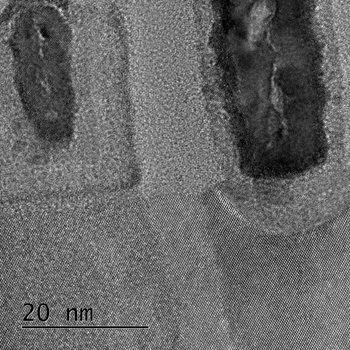
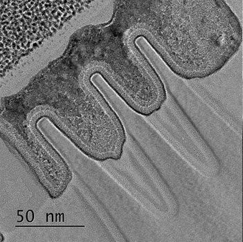
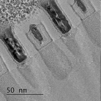
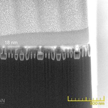
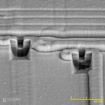
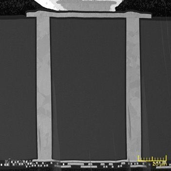
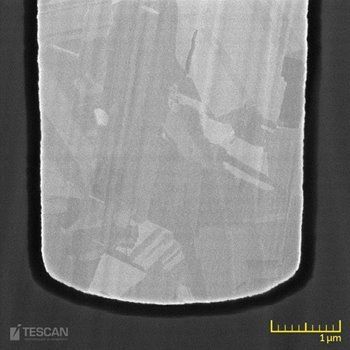
Vías a través de Silicon
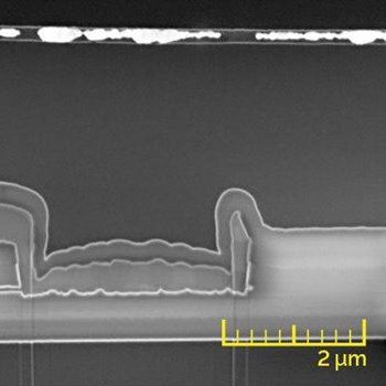
Vías a través de Silicio (TSVs) es una tecnología avanzada de interconexión en en chips 3D, crucial para el empaquetado de integración en chips 3D. Los TSV interconectan verticalmente capas de pastillas o dados mejorando el rendimiento eléctrico, menor consumo y factor de forma para circuitos integrados 3D.
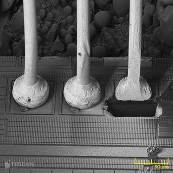
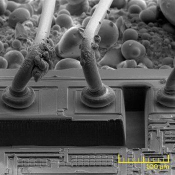
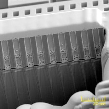
Alambres de unión
El uso de alambres de unión ultra finos de cobre y oro continúan siendo el método más utilizado para crear interconexiones en módulos de chips de alta densidad en la industria microelectrónica y de semiconductores.
Pantallas
El desarrollo de pantallas ha progresado rápidamente en los últimos años lo cual ha resultado en pantallas táctiles de alta calidad que ofrecen imágenes nítidas y brillantes, amplios ángulos de visión, y vivos colores.
MEMS
Los sistemas micro-electro-mecánicos (MEMS) son una tecnología que se puede definir generalmente como elementos mecánicos y electromecánicos miniaturizados comúnmente hechos con substrato de Si y fabricados por medio de fotolitografía e impresión o grabado químico.
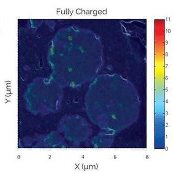
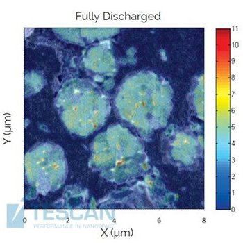
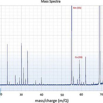
Baterías
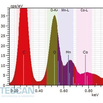
Un gran número de investigaciones en la industria de las baterías tiene lugar cada día con el fin de desarrollar los sistemas de almacenamiento de energía del futuro, una tarea que sigue siendo uno de los desafíos tecnológicos de más relevancia actual. Esto requiere técnicas analíticas capaces de diferenciar estados químicos con alta sensibilidad y alta resolución espacial.
Equipos TESCAN para SEMICONDUCTORES
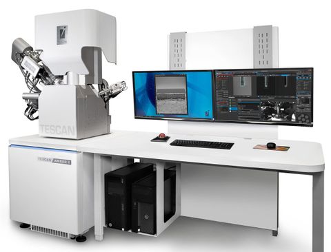
TESCAN SOLARIS
Banco de trabajo de nanofabricación avanzada para su laboratorio de investigación.
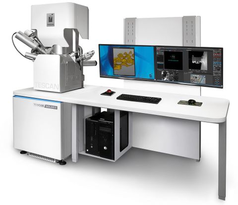
TESCAN SOLARIS X
Una plataforma Plasma FIB-SEM para seccionamiento profundo y la más alta resolución para el análisis de fallas en microelectrónica.